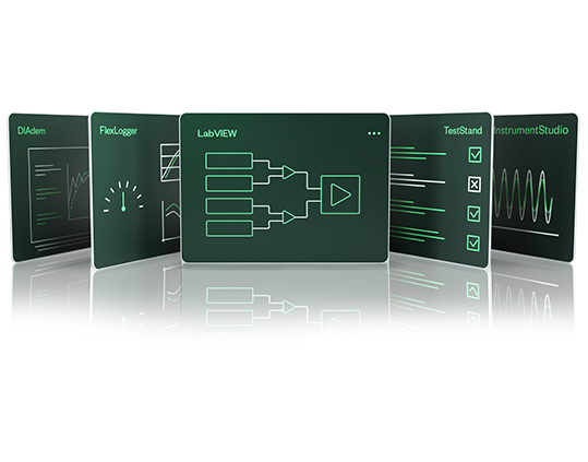
LabVIEW has what you need to build automated test systems, fast. Outpace the competition with LabVIEW. Unlike other solutions:
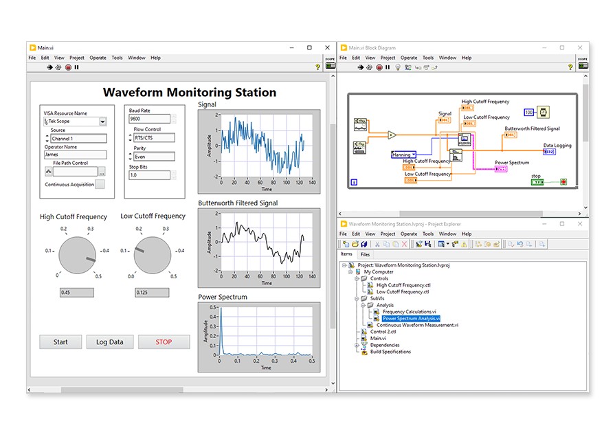
LabVIEW can connect to any instrument, regardless of vendor
LabVIEW has a native user interface for monitoring and controlling test
LabVIEW has thousands of engineering analysis functions
LabVIEW works with popular programming languages, such as Python, C, and .NET