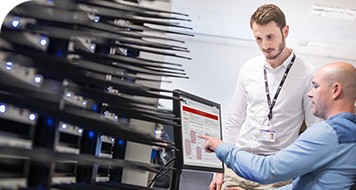

Maximize productivity and reduce costs with NI services. As your trusted partner and expert connector, we’re here to help you Engineer Ambitiously™.

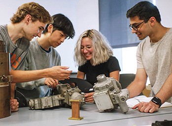
Whether in the classroom or the lab, today’s students and researchers look to increase their rate of discovery and innovation. NI provides solutions that address challenges from the classroom to leading fields of research like wireless communications. We partner with education experts to develop the right tools to help students understand problems and build real solutions faster than ever.

We understand that researchers need solutions that help push the boundaries of discovery. Driven by challenges and trending tech revolutionizing wireless communications, transportation, and energy, engineering educators prepare students to become the innovators of tomorrow. Whether in the lab or the classroom, NI hardware and software supports an engaging, hands-on curriculum that inspires students and puts theory into practice to accelerate discovery.
NI Services
Maximize productivity and reduce costs with NI services. As your trusted partner and expert connector, we’re here to help you Engineer Ambitiously™.